- 您现在的位置:买卖IC网 > Sheet目录471 > MAX2029ETP+T (Maxim Integrated)IC MIXER UP/DOWN HI LIN 20-TQFN
�� �
�
�High-Linearity,� 815MHz� to� 1000MHz� Upconversion/�
�Downconversion� Mixer� with� LO� Buffer/Switch�
�and� LO2� inputs� are� internally� matched� to� 50� Ω� ,� requiring�
�an� 82pF� DC-blocking� capacitor� at� each� input.�
�A� two-stage� internal� LO� buffer� allows� a� wide� input-�
�power� range� for� the� LO� drive.� All� guaranteed� specifica-�
�tions� are� for� a� -3dBm� to� +3dBm� LO� signal� power.� The�
�on-chip� low-loss� balun,� along� with� an� LO� buffer,� drives�
�the� double-balanced� mixer.� All� interfacing� and� match-�
�ing� components� from� the� LO� inputs� to� the� IF� outputs�
�are� integrated� on-chip.�
�High-Linearity� Mixer�
�The� core� of� the� MAX2029� is� a� double-balanced,� high-�
�performance� passive� mixer.� Exceptional� linearity� is� pro-�
�vided� by� the� large� LO� swing� from� the� on-chip� LO� buffer.�
�Differential� IF�
�The� MAX2029� mixer� has� a� DC� to� 250MHz� IF� frequency�
�range.� Note� that� these� differential� ports� are� ideal� for� pro-�
�viding� enhanced� IIP2� performance.� Single-ended� IF�
�applications� require� a� 1:1� balun� to� transform� the� 50� Ω� dif-�
�ferential� IF� impedance� to� 50� Ω� single-ended.� Including�
�the� balun,� the� IF� return� loss� is� better� than� 15dB.� The� dif-�
�ferential� IF� is� used� as� an� input� port� for� upconverter� oper-�
�ation.� The� user� can� use� a� differential� IF� amplifier� following�
�the� mixer,� but� a� DC� block� is� required� on� both� IF� pins.�
�Applications� Information�
�Input� and� Output� Matching�
�factory� for� details.� If� the� ±1%� bias� resistor� values� are�
�not� readily� available,� substitute� standard� ±5%� values.�
�Layout� Considerations�
�A� properly� designed� PCB� is� an� essential� part� of� any�
�RF/microwave� circuit.� Keep� RF� signal� lines� as� short� as�
�possible� to� reduce� losses,� radiation,� and� inductance.�
�For� the� best� performance,� route� the� ground-pin� traces�
�directly� to� the� exposed� pad� under� the� package.� The�
�PCB� exposed� pad� MUST� be� connected� to� the� ground�
�plane� of� the� PCB.� It� is� suggested� that� multiple� vias� be�
�used� to� connect� this� pad� to� the� lower-level� ground�
�planes.� This� method� provides� a� good� RF/thermal� con-�
�duction� path� for� the� device.� Solder� the� exposed� pad� on�
�the� bottom� of� the� device� package� to� the� PCB.� The�
�MAX2029� evaluation� kit� can� be� used� as� a� reference� for�
�board� layout.� Gerber� files� are� available� upon� request� at�
�www.maxim-ic.com.�
�Power-Supply� Bypassing�
�Proper� voltage-supply� bypassing� is� essential� for� high-�
�frequency� circuit� stability.� Bypass� each� V� CC� pin� with�
�the� capacitors� shown� in� the� Typical� Application� Circuit.�
�See� Table� 1.�
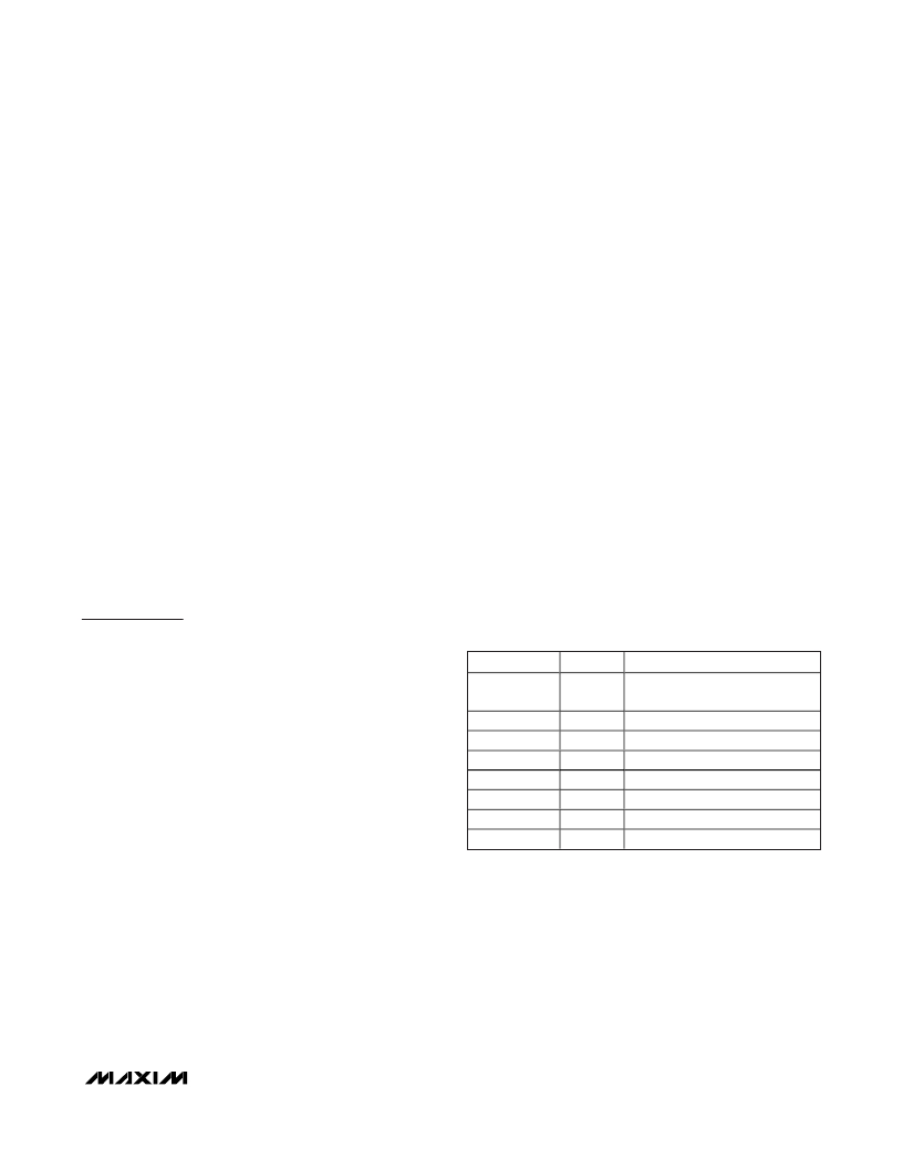
�Table� 1.� Typical� Application� Circuit�
�Component� List�
�The� RF� and� LO� inputs� are� internally� matched� to� 50� Ω� .� No�
�matching� components� are� required.� As� a� downconvert-�
�er,� the� return� loss� at� the� RF� port� is� typically� better� than�
�15dB� over� the� entire� input� range� (815MHz� to� 1000MHz),�
�and� return� loss� at� the� LO� ports� are� typically� 15dB�
�(570MHz� to� 850MHz).� RF� and� LO� inputs� require� only�
�DC-blocking� capacitors� for� interfacing.�
�An� optional� L-C� bandpass� filter� (BPF)� can� be� installed� at�
�the� RF� port� to� improve� upconverter� performance.� See�
�the� Typical� Application� Circuit� and� Typical� Operating�
�Characteristics� for� upconverter� operation� with� an� L-C�
�COMPONENT�
�C1,� C2,� C7,� C8,�
�C10,� C11,� C12�
�C3,� C6,� C9�
�C4*�
�C5**�
�L1*�
�R1�
�T1�
�VALUE�
�82pF�
�10nF�
�4.7pF�
�3.3pF�
�4.7nH�
�523� Ω�
�1:1�
�DESCRIPTION�
�Microwave� capacitors� (0603)�
�Microwave� capacitors� (0603)�
�Microwave� capacitor� (0603)�
�Microwave� capacitor� (0603)�
�Inductor� (0603)�
�±1%� resistor� (0603)�
�IF balun M/A-COM: MABAES0029�
�BPF� tuned� for� 920MHz� RF� frequency.� Performance� can�
�U1�
�MAX2029� Maxim� IC�
�be� optimized� at� other� frequencies� by� choosing� different�
�values� for� L1� and� C4.� Removing� L1� and� C4� altogether�
�results� in� a� broader� match,� but� performance� degrades.�
�Contact� factory� for� details.�
�The� IF� output� impedance� is� 50� Ω� (differential).� For� eval-�
�uation,� an� external� low-loss� 1:1� (impedance� ratio)� balun�
�transforms� this� impedance� to� a� 50� Ω� single-ended� out-�
�put� (see� the� Typical� Application� Circuit).�
�Bias� Resistor�
�Bias� current� for� the� LO� buffer� is� optimized� by� fine� tun-�
�ing� resistor� R1.� If� reduced� current� is� required� at� the�
�expense� of� performance,� contact� the�
�*C4� and� L1� installed� only� when� mixer� is� used� as� an� upconverter.�
�**C5� installed� only� when� mixer� is� used� as� a� downconverter.�
�Exposed� Pad� RF/Thermal� Considerations�
�The� exposed� paddle� (EP)� of� the� MAX2029’s� 20-pin� thin�
�QFN-EP� package� provides� a� low-thermal-resistance�
�path� to� the� die.� It� is� important� that� the� PCB� on� which� the�
�MAX2029� is� mounted� be� designed� to� conduct� heat�
�from� the� EP.� In� addition,� provide� the� EP� with� a� low-�
�inductance� path� to� electrical� ground.� The� EP� MUST� be�
�soldered� to� a� ground� plane� on� the� PCB,� either� directly�
�or� through� an� array� of� plated� via� holes.�
�______________________________________________________________________________________�
�13�
�发布紧急采购,3分钟左右您将得到回复。
相关PDF资料
MAX2031EVKIT
EVAL KIT FOR MAX2031
MAX2032ETP+
IC MIXER UP/DOWN CONVER 20TQFN
MAX2034CTM+
IC AMP LOW NOISE QUAD 48-TQFN
MAX2035EVKIT
EVAL KIT FOR MAX2035
MAX2039ETP+D
IC MIXER UP/DWN HI LIN 20-TQFN
MAX2039EVKIT
EVAL KIT FOR MAX2039
MAX2041ETP+T
IC MIXER UP/DWN HI LIN 20-TQFN
MAX2041EVKIT
EVAL KIT FOR MAX2041
相关代理商/技术参数
MAX2029ETP-T
功能描述:射频混合器 .815GHz-1GHz Up/Down Mixer RoHS:否 制造商:NXP Semiconductors 频率范围: 转换损失——最大: 工作电源电压:6 V 最大工作温度:+ 85 C 最小工作温度:- 40 C 安装风格:Through Hole 封装 / 箱体:PDIP-8 封装:Tube
MAX2029EVKIT
制造商:Maxim Integrated Products 功能描述:HIGH-LINEARITY 815MHZ TO 1000MHZ U - Rail/Tube
MAX202C
制造商:TI 制造商全称:Texas Instruments 功能描述:5-V DUAL RS-232 LINE DRIVER/RECEIVER WITH +-15KV ESD PROTECTION
MAX202C/D
功能描述:RS-232接口集成电路 RoHS:否 制造商:Exar 数据速率:52 Mbps 工作电源电压:5 V 电源电流:300 mA 工作温度范围:- 40 C to + 85 C 安装风格:SMD/SMT 封装 / 箱体:LQFP-100 封装:
MAX202C/D DIE
制造商:Maxim Integrated Products 功能描述:
MAX202CD
功能描述:RS-232接口集成电路 5V Dual Line Driver/Receiver RoHS:否 制造商:Exar 数据速率:52 Mbps 工作电源电压:5 V 电源电流:300 mA 工作温度范围:- 40 C to + 85 C 安装风格:SMD/SMT 封装 / 箱体:LQFP-100 封装:
MAX202CD
制造商:Texas Instruments 功能描述:LINE DRIVER DUAL 5V SMD SOIC16
MAX202CD
制造商:Texas Instruments 功能描述:IC RS-232 TRANSCEIVER 5V SOIC-16 制造商:Texas Instruments 功能描述:IC, RS-232 TRANSCEIVER, 5V, SOIC-16